AI’s Next Bottleneck: Chip Packaging Delays Highlight U.S.–Asia Dependency
As artificial intelligence drives unprecedented demand for advanced semiconductors, a lesser-known stage in chip production—advanced packaging—is emerging as a critical bottleneck.
Even when chips are manufactured in the U.S., they often must be sent overseas, primarily to Taiwan, for packaging before they can be used. This step, which integrates chips into systems that can interact with real-world devices, is currently dominated by Asian manufacturers, with limited global capacity.
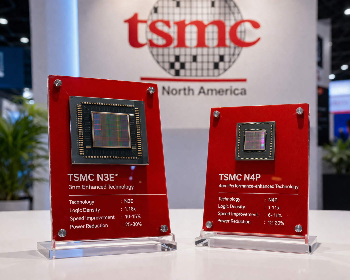
Taiwan Semiconductor Manufacturing Company (TSMC) leads the space with its advanced packaging technology known as CoWoS (Chip on Wafer on Substrate), which is seeing explosive growth. According to company executives, demand for this technology is increasing at an annual rate of about 80%, fueled largely by AI workloads.
Major AI players like Nvidia have already secured a significant share of this capacity, leaving limited availability for others. This has intensified concerns that packaging—not chip fabrication—could become the next major constraint in scaling AI infrastructure.
While the U.S. has made strides in chip manufacturing, including new fabrication plants in Arizona, most chips still travel back to Taiwan for final packaging. TSMC is now working to build packaging facilities in the U.S., but timelines remain unclear.
Intel is positioning itself as an alternative, offering advanced packaging services and working with companies like Amazon and Cisco. It is also gaining attention after Elon Musk selected Intel to package custom chips for ventures including SpaceX, Tesla, and xAI.
Advanced packaging has become increasingly important as chip design evolves. Instead of relying on a single chip, modern AI systems combine multiple components—such as processors and memory—into tightly integrated units like GPUs. This requires sophisticated packaging techniques to ensure high-speed communication and efficiency.
Experts say the shift represents an extension of Moore’s Law into three dimensions, with new approaches like 2.5D and 3D packaging enabling higher performance gains. Companies are also exploring innovations such as hybrid bonding to further improve speed and energy efficiency.
Despite growing investment, supply remains tight. Industry leaders warn that without significant capital expenditure in packaging infrastructure, the AI boom could face delays—even if chip manufacturing capacity keeps expanding.
The situation underscores a broader challenge: while the U.S. is investing heavily in semiconductor production, critical parts of the supply chain still rely heavily on Asia, making advanced packaging a key battleground in the future of AI hardware.